Tunable electronic structure in stained two dimensional van der Waals g-C2N/XSe2 (X = Mo,W) heterostructures |
| |
| Affiliation: | 1. Tianjin Key Laboratory of Film Electronic&Communicate Devices, School of Electrical and Electronic Engineering, Tianjin University of Technology, Tianjin 300384, China;2. Tianjin Key Laboratory of Low Dimensional Materials Physics and Preparation Technology, School of Science, Tianjin University, Tianjin 300354, China;1. School of Computer Science, Jiangxi University of Traditional Chinese Medicine, Nanchang 330004, China;2. School of Science, East China Jiaotong University, Nanchang 330013, China;1. School of Materials Science and Engineering, Shandong Jianzhu University, 250101 Jinan, PR China;2. Science and Technology on Power Beam Processes Laboratory, Beijing Key Laboratory of High Power Beam Additive Manufacturing Technology and Equipment, Aeronautical Key Laboratory for Additive Manufacturing Technologies, AVIC Manufacturing Technology Institute, 100024 Beijing, PR China |
| |
| Abstract: | 
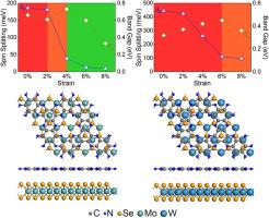
The electronic structure of the strained g-C2N/XSe2 (X=Mo, W) van der Waals heterostructures are investigated by first-principles calculations. The g-C2N/MoSe2 heterostructure is an indirect band gap semiconductor at a strain from 0% to 8%, where its band gap is 0.66, 0.61, 0.73, 0.60 and 0.33 eV. At K point, the spin splitting is 186, 181, 39, 13 and 9 meV, respectively. For g-C2N/WSe2 heterostructures, the band gap is 0.32, 0.37, 0.42, 0.45 and 0.36 eV, and the conduction band minimum is shifted from Г-M region to K-Г region as the strain increases from 0% to 8%. Its spin splitting monotonically decreases as a strain raises to 8%, which is 445, 424, 261, 111 and 96 meV, respectively. Moreover, at a strain less than 4%, the conduction band mainly comes from g-C2N, but it comes from XSe2 (X=Mo, W) above 6%. Our results show that the g-C2N/XSe2 heterostructures have tunable electronic structures, which makes it a potential candidate for novel electronic devices. |
| |
| Keywords: | Two dimensional semiconductor Transition metal dichalcogenide Strain effect Spin splitting |
| 本文献已被 ScienceDirect 等数据库收录! |
|

